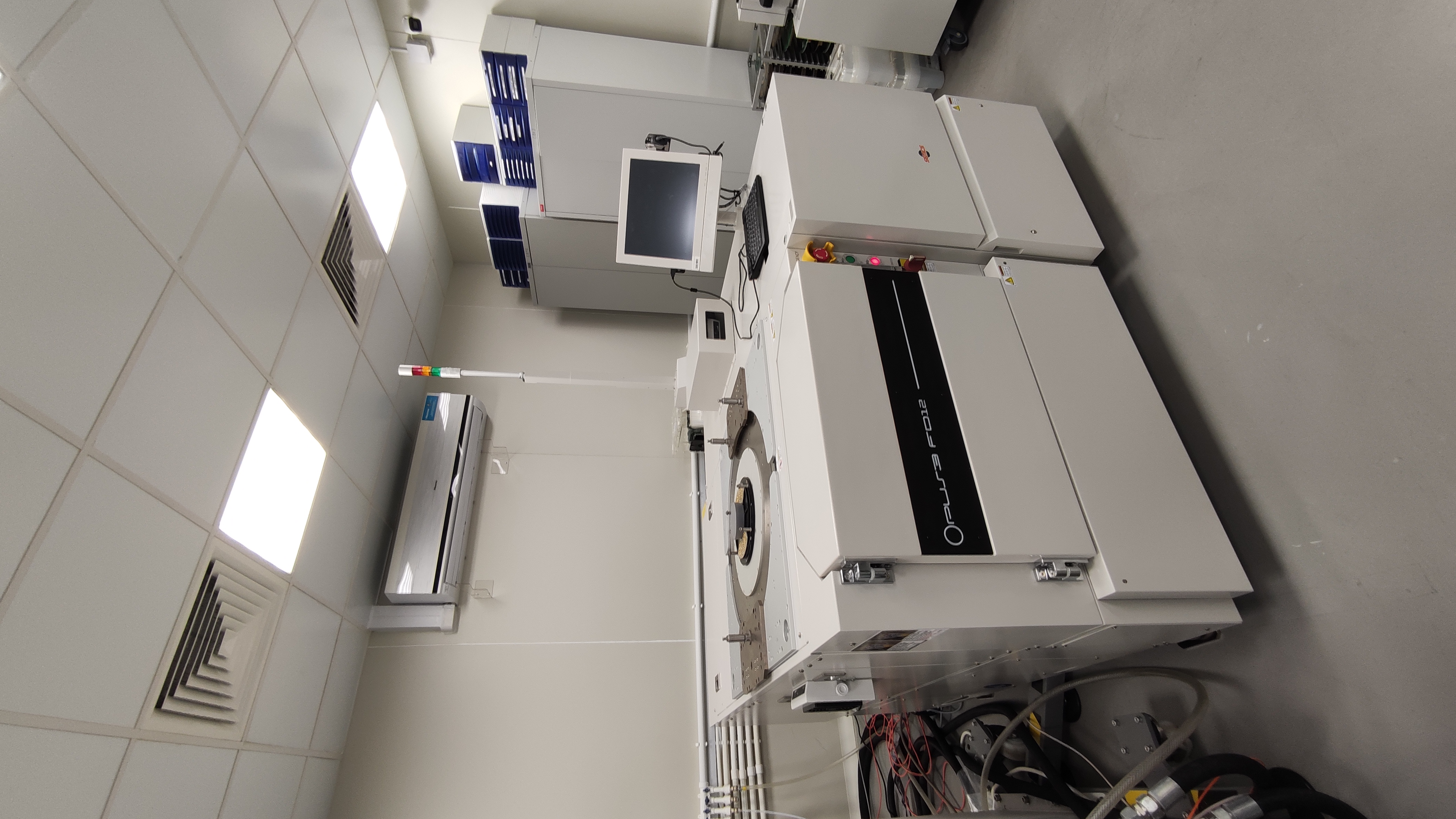
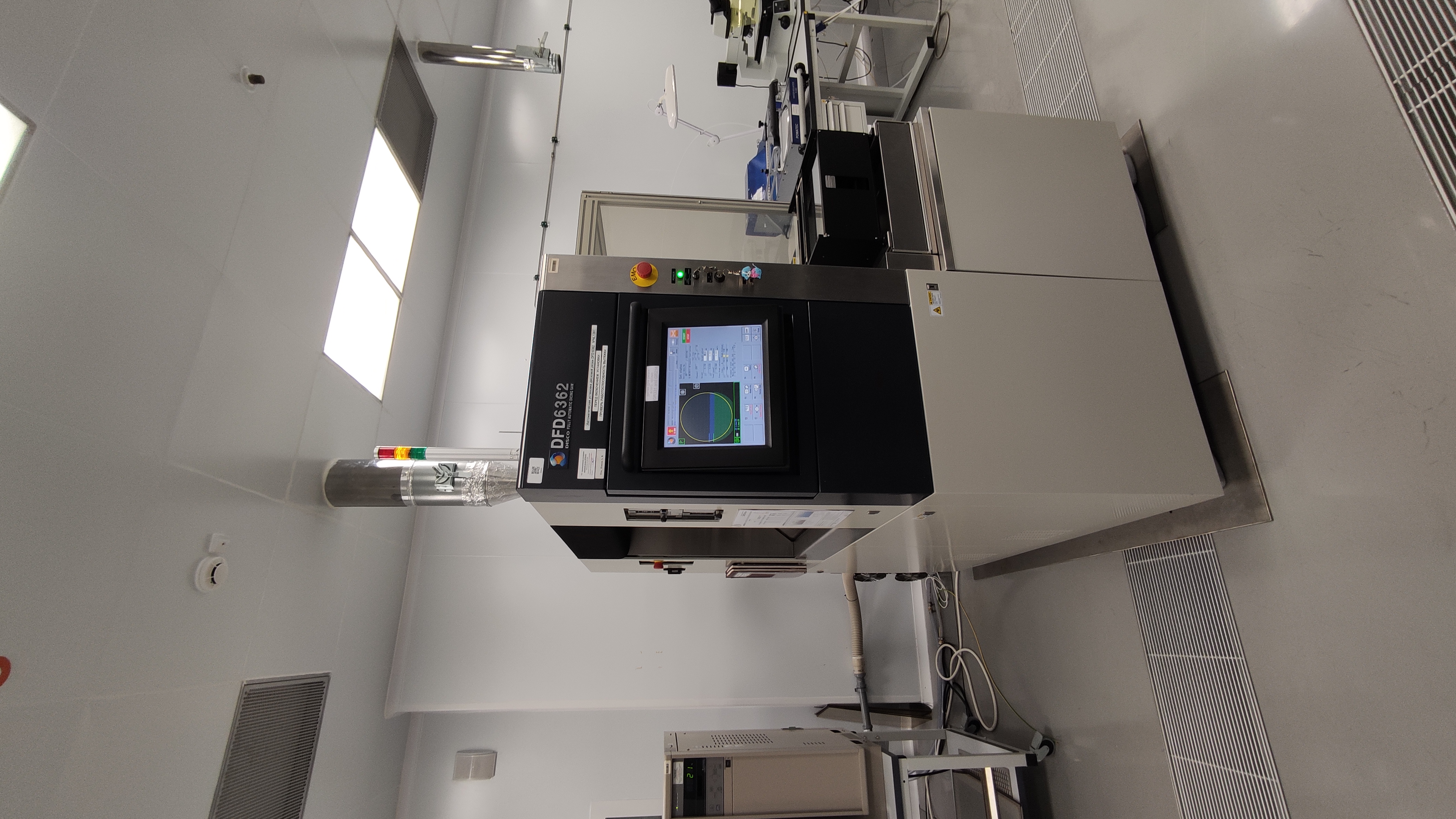
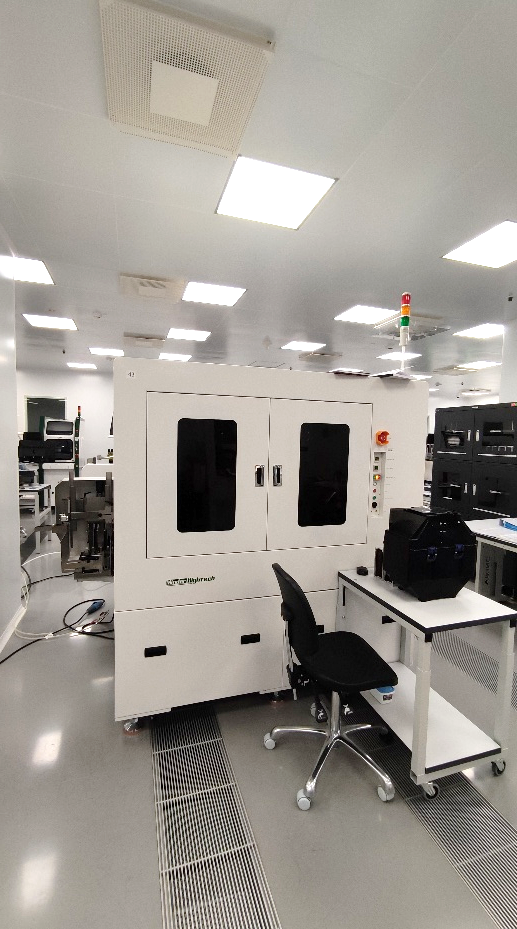
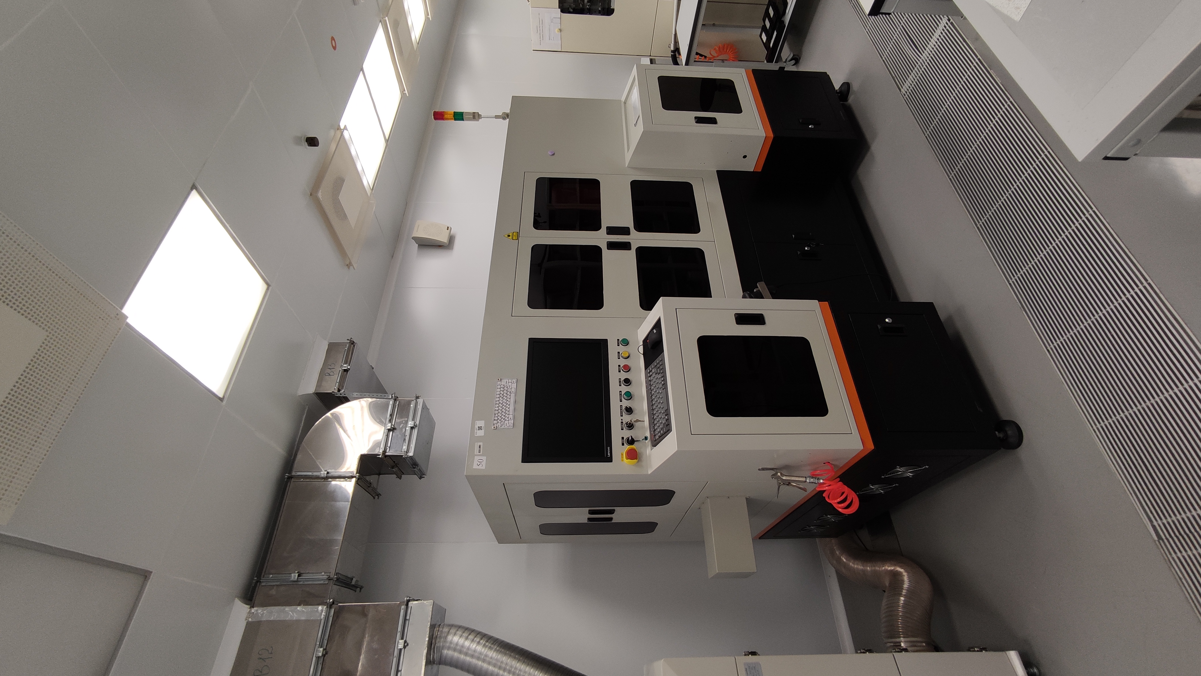
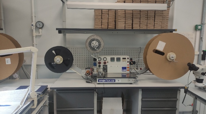
From wafer probing through final packaging of finished integrated circuits.
Electrical parameter measurement on wafers
High-precision diamond blade wafer dicing.
Precise placement and secure die attachment.
Durable high-contrast product marking.
Complete assembly, encapsulation and testing cycle.